msxnet > Technical Info > Konami SCC Sound Chip
The SCC is a wavetable sound chip, just like the Gravis Ultra Sound, Sound Blaster (AWE)32 and Moonsound. They all have memory (tables), in which samples (waves) are stored. The samples are played back looped. The speed with which the samples are played, determines the frequency of the tone. A modern wavetable sound module usually has over a megabyte of memory, while the SCC has 128 bytes of memory.
List of what the SCC ICs says:
Clay Cowgill explains: the last digits aren't really a serial number, but rather a date code and fabrication location/lot numbers. The format is Year, Week, Info, so 8740AAA is:
1987, 40th week (probably early November), AAA code (that would be manufacturer specific, but it probably tells what factory made it, what wafer batch it was from, what process line it was on, etc.)
You'll notice that the first two digits stay between 87-88 (they seem to have made all the chips between 1987 and 1988) and the next two digits are between 01-52 (only 52 weeks in a year).
Otherwise, all the chips you listed should be identical. (You could swap them and they'd still work the same in theory-- they were just made at different times.)
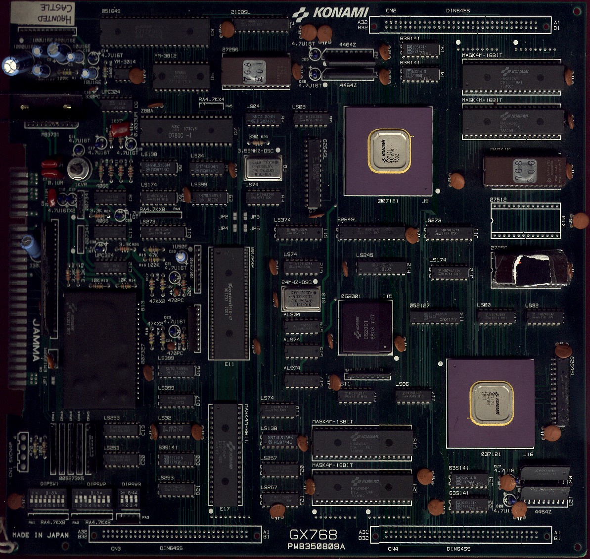
This SCC was also used in several arcade games made by Konami. As far as I know they are: Haunted Castle, City Bomber, Hexion, Nyan Nyan Panic. All of these are emulated by mame. Apart from the SCC (known as K051649 in MAME) they also use an YM3812 (OPL2) for music and another chip for samples.
I've got the Haunted Castle PCB, Levien van Zon has made an excellent scan of it. To the left of the SCC (which is at the top-left) you can see the resistors packed into one device (which is for D/A conversion). You can also see the YM3812 (OPL2) and the Z80A.
The SCC has five channels. There are four functions for each channel:
Just like the bank select registers, the SCC is accessed through memory mapped I/O, and not through I/O ports. If you write xx111111b (3Fh, bits 7 and 6 are ignored) to bank select register 3 (memory area 9000h to 97FFh, see megaROM mappers for more information), the SCC can be accessed through memory area from 9800h to 9FFFh.
The register structure is similar to the PSG.
| Address | Function |
|---|---|
| 9800h - 981Fh | waveform channel 1 |
| 9820h - 983Fh | waveform channel 2 |
| 9840h - 985Fh | waveform channel 3 |
| 9860h - 987Fh | waveform channel 4 and 5 |
| 9880h - 9881h | frequency channel 1 |
| 9882h - 9883h | frequency channel 2 |
| 9884h - 9885h | frequency channel 3 |
| 9886h - 9887h | frequency channel 4 |
| 9888h - 9889h | frequency channel 5 |
| 988Ah | volume channel 1 |
| 988Bh | volume channel 2 |
| 988Ch | volume channel 3 |
| 988Dh | volume channel 4 |
| 988Eh | volume channel 5 |
| 988Fh | on/off switch channel 1 to 5 |
| 9890h - 989Fh | same as 9880h to 988Fh |
| 98A0h - 98DFh | no function |
| 98E0h - 98FFh | test register |
As you may have noticed, channel 4 shares its waveform with channel 5. The SCC+ has five waveforms so each channel has it's own waveform. See SCC+ Sound Cartridge for more information.
The waveform is made up of 32, signed (two's complement) bytes. The waveform represents the actual form of the tone the sound chip produces. It's played back from byte 0 to 31, and then again from 0 to 31, etc. A value of 0 means no amplitude. From 1 to 127 results in an increasingly higher amplitude. From -1 to -128 (FFh to 80h) results in an increasingly higher negative amplitude.
The frequency is stored the same way as in the PSG. The first byte contains bits 0 to 7 from the frequency. Bits 0 to 3 of the second byte contain bits 8 to 11 of the frequency. Bits 4 to 7 of the second byte are ignored. Remember that the value you enter is a period: a higher value gives a lower frequency.
The formula for calculating the frequency of the tone is the same as from the PSG:
               fclock
   ftone = -------------
            32 * (TP + 1)
fclock is the clock frequency of the computer. 3,579,545 Hz
ftone is the frequency of the channel
TP is the value in the frequency registers
The volume is stored in the same way as in the PSG, though it does not support envelopes. Bits 0 to 3 contain a volume of 0 to 15, and bits 7 to 4 are ignored. A volume of 0 is silent, and a volume of 15 is maximum volume.
The on/off switch register switches the different channels on or off. Set the associated bit high for a channel to activate it. It has the following structure:
| Bit | 7 | 6 | 5 | 4 | 3 | 2 | 1 | 0 |
|---|---|---|---|---|---|---|---|---|
| Channel | none | none | none | 5 | 4 | 3 | 2 | 1 |
This register is not used by Konami. All the addresses in the memory area (98E0h - 98FFh) refer to the same register. It is set a different memory area in the SCC+ (Sound Cartridge).
| Bit | 7 | 6 | 5 | 4 | 3 | 2 | 1 | 0 |
|---|---|---|---|---|---|---|---|---|
| Function | ROTAT1 | ROTAT0 | CNTRES | FREFO2 | FREFO1 | FREFO0 | FMLT1 | FMLT0 |
The default value is 0.
The ROTAT bits select which waves will be rotating. If ROTAT0 is set the waves for channels 1, 2 and 3 will rotate at the speed of their channel's ftone, the shared wave for channels 4 and 5 will rotate at the speed of the ftone for channel 5. If ROTAT1 is set only the shared wave for channels 4 and 5 will rotate at the speed of the ftone for channel 4. If both ROTAT0 and ROTAT1 are set only the waves for channels 1, 2 and 3 will rotate at the speed of their channel's ftone.
The CNTRES bit will cause the wave counter for a channel to restart every time the tone value for that channel changes.
The FREFO bits cause a certain internal signal to be output directly to the
outside world through the FREF/TEST pin:
000: Channel 1 Frequency Counter
001: Channel 2 Frequency Counter
010: Channel 3 Frequency Counter
011: Channel 4 Frequency Counter
100: Channel 5 Frequency Counter
101: Channel 4 & 5 RAM Address Select Bit 0
110: Channel 4 & 5 RAM Address Select Bit 1
111: Always low
The FMLT bits change the frequency of all the channels. If FMLT0 is set all
the frequencies are multiplied by 256. If FMLT1 is set all frequencies are
multiplied by 16, overriding the 256 multiplication.
(Most frequencies are shifted out of hearing range, except if you set the
frequency to minimum (TP = FFFh), then you'll hear something.)
The memory area from 9800h to 987Fh behaves as RAM. The memory area from 9880h to 98FFh is write only; if you read it, it'll always return FFh.
The memory area from 9900h to 99FFh has exactly the same function as from 9800h to 98FFh. The same accounts for the area from 9A00h to 9AFFh, and so on to the area from 9F00h to 9FFFh. This behaviour can be easily be explained: the SCC/Mapper does not process address line A8 - A10, thus it cannot distinguish 9900h from 9800h, or 9F00h from 9800h. See pinouts.txt for more info.
The memory area from 8000h to 97FFh is a part of the ROM as you would expect it to be.
How do you know in which slot the SCC is? One way is to search the slots for cartridge with the 'AB' code that can be removed by writing a value other than 0 to the bank select register. However, in some cartridges the ROM is disabled; you won't find the 'AB' code. A better way is to search for a slot that contains ROM, and contains RAM at 9800h - 987Fh after writing 3Fh to 9000h. This will also work on the SCC+.
When reading the test register, it will return FFh, which isn't weird, because the register is write only. However, for some reason that value will also be written to the test register, causing the wave rotation to start. Writing 0 to the test register will restore the SCC to its original functionality.
pinouts.txt - local file
Disabling Game in Konami SCC Cartridges - local file
CJS documents page (archive.org) - Dutch only!
IKASCC GitHub project - a die shot based cycle-accurate Konami SCC core
BiFi <bifi@msxnet.org>.